- 您现在的位置:买卖IC网 > Sheet目录2007 > MAX11101EUB+ (Maxim Integrated Products)IC ADC 14BIT SRL 200KSPS 10UMAX
Maxim Integrated Products 11
MAX11101
14-Bit, +5V, 200ksps ADC with 10A Shutdown
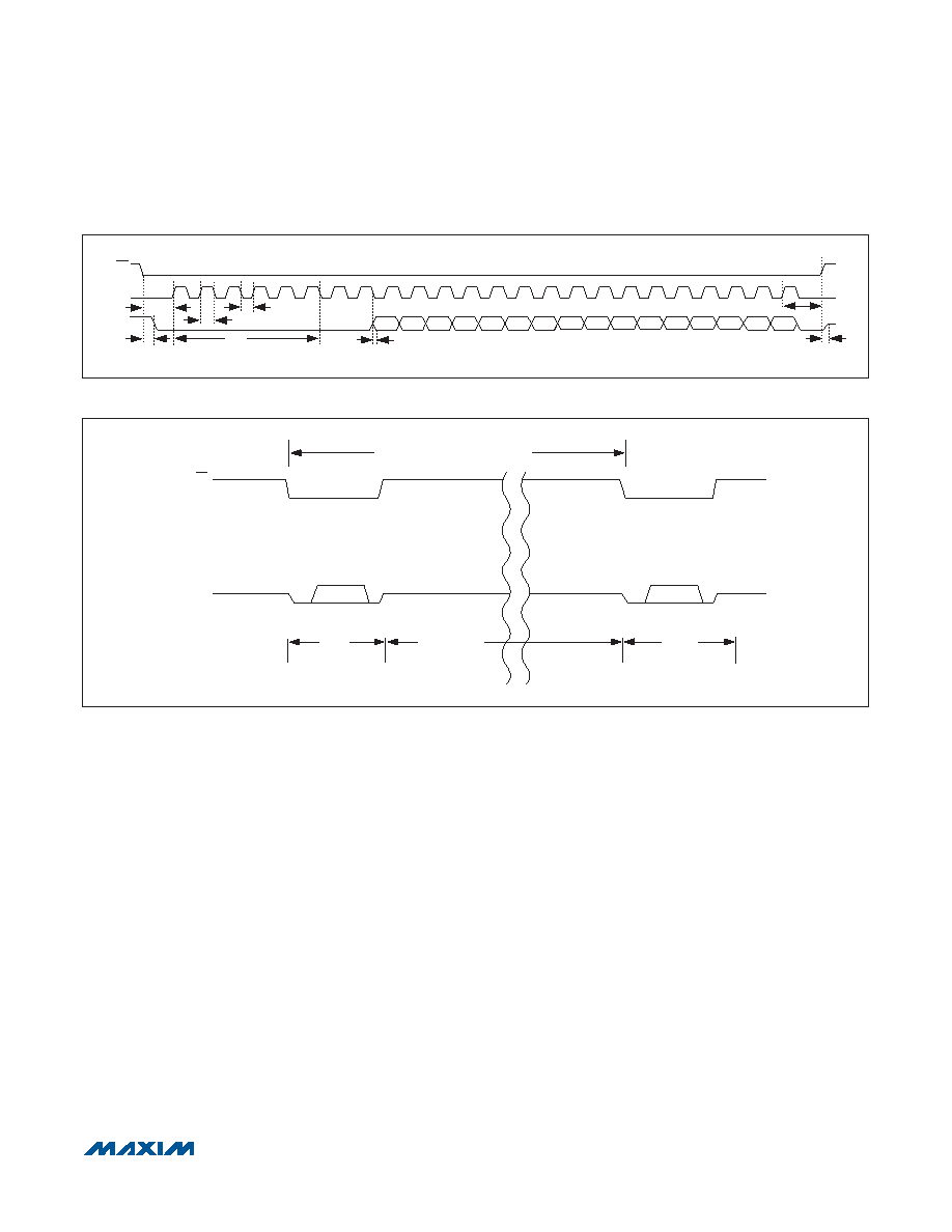
A CS falling edge initiates an acquisition sequence. The
analog input is stored in the capacitive DAC, DOUT
changes from high impedance to logic-low, and the ADC
begins to convert after the sixth clock cycle. SCLK drives
the conversion process and shifts out the conversion
result on DOUT.
SCLK begins shifting out the data (MSB first) after the fall-
ing edge of the 8th SCLK pulse. Twenty-four falling clock
edges are needed to shift out the eight leading zeros, 14
data bits, and 2 sub-bits (S1 and S0). Extra clock pulses
occurring after the conversion result has been clocked
out, and prior to the rising edge of CS, produce trail-
ing zeros at DOUT and have no effect on the converter
operation.
Force CS high after reading the conversion’s LSB to
reset the internal registers and place the MAX11101 in
shutdown. For maximum throughput, force CS low again
to initiate the next conversion immediately after the speci-
fied minimum time (tCSW).
Note: Forcing CS high in the middle of a conversion
immediately aborts the conversion and places the
MAX11101 in shutdown.
Figure 6. External Timing Diagram
Figure 7. Shutdown Sequence
CS
SCLK
20
16
24
12
14
8
6
DOUT
D13 D12 D11 D10
D9
D8
D7
S1
S0
D6
D3
D2
D1
D0
D5
D4
tCSH
tTR
tDO
tACQ
tCSS
tCH
tCL
tDN
COMPLETE CONVERSION SEQUENCE
CONVERSION 0
CONVERSION 1
POWERED UP
POWERED DOWN
DOUT
CS
发布紧急采购,3分钟左右您将得到回复。
相关PDF资料
MAX11102AUB+
IC ADC 12BIT SPI/SRL 10UMAX-EP
MAX1111CPE+
IC ADC 8BIT LP 16-DIP
MAX1113CPE+
IC ADC 8BIT LP 16-DIP
MAX1116EKA+T
IC ADC 8BIT SERIAL SOT23-8
MAX11201BEUB+T
IC ADC 24BIT SRL 13.75SPS 10UMAX
MAX11202BEUB+T
IC ADC 24BIT SRL 13.75SPS 10UMAX
MAX11210EEE+T
ADC 24BIT 4WIRE SPI 16-QSOP
MAX11212BEUB+T
IC ADC 18BIT SRL 13.75SPS 10UMAX
相关代理商/技术参数
MAX11101EUB+T
功能描述:模数转换器 - ADC 14-Bit 5V 200ksps w/10uA Shutdown RoHS:否 制造商:Texas Instruments 通道数量:2 结构:Sigma-Delta 转换速率:125 SPs to 8 KSPs 分辨率:24 bit 输入类型:Differential 信噪比:107 dB 接口类型:SPI 工作电源电压:1.7 V to 3.6 V, 2.7 V to 5.25 V 最大工作温度:+ 85 C 安装风格:SMD/SMT 封装 / 箱体:VQFN-32
MAX11101EWC
制造商:MAXIM 制造商全称:Maxim Integrated Products 功能描述:14-Bit, +5V, 200ksps ADC with 10μA Shutdown
MAX11101EWC+
制造商:MAXIM 制造商全称:Maxim Integrated Products 功能描述:14-Bit, 5V, 200ksps ADC with 10??A Shutdown
MAX11101EWC+T
功能描述:模数转换器 - ADC 14-Bit 5V 200ksps w/10uA Shutdown RoHS:否 制造商:Texas Instruments 通道数量:2 结构:Sigma-Delta 转换速率:125 SPs to 8 KSPs 分辨率:24 bit 输入类型:Differential 信噪比:107 dB 接口类型:SPI 工作电源电压:1.7 V to 3.6 V, 2.7 V to 5.25 V 最大工作温度:+ 85 C 安装风格:SMD/SMT 封装 / 箱体:VQFN-32
MAX11102
制造商:MAXIM 制造商全称:Maxim Integrated Products 功能描述:2Msps/3Msps, Low-Power, Serial 12-/10-/8-Bit ADCs
MAX11102_11
制造商:MAXIM 制造商全称:Maxim Integrated Products 功能描述:2Msps/3Msps, Low-Power, Serial 12-/10-/8-Bit ADCs 2.2V to 3.6V Supply Voltage
MAX11102_1108
制造商:MAXIM 制造商全称:Maxim Integrated Products 功能描述:2Msps/3Msps, Low-Power, Serial 12-/10-/8-Bit ADCs
MAX11102ATB
制造商:MAXIM 制造商全称:Maxim Integrated Products 功能描述:2Msps/3Msps, Low-Power, Serial 12-/10-/8-Bit ADCs 2.2V to 3.6V Supply Voltage